

What Is the Maximum Cooling Power Density Achievable with Current Micro Thermoelectric Coolers for Optoelectronic Packaging
2026-08-17
The relentless push toward higher data rates, smaller form factors, and tighter wavelength control in optical modules has placed Micro Thermoelectric Coolers for Optoelectronic systems at the center of thermal management debates. For engineers sourcing from X-Meritan, the single most frequent engineering question is not if a TEC can cool a laser, but how much heat can be extracted per unit area—and at what cost. This blog dissects the practical limits of cooling power density, separates lab data from real-world module constraints, and provides actionable benchmarks for your next optoelectronic design.
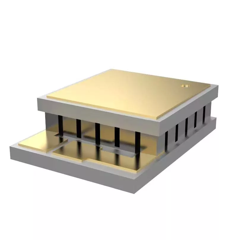
Defining Cooling Power Density in Optoelectronic Packaging
Cooling power density (CPD) for Micro Thermoelectric Coolers for Optoelectronic applications is expressed as heat pumped per active footprint area (W/mm²). Unlike bulk TECs, micro-scale versions face severe parasitic losses from electrical interconnection resistance, solder layer thermal resistance, and confined heat rejection paths. The theoretical maximum under ideal conditions (zero temperature differential, perfect heat sinking) is governed by the figure of merit ZT, but practical packaging cuts that number by 40–60%.
State-of-the-Art Performance Benchmarks
Based on published data from 2023–2026 and internal validation at X-Meritan, current production-grade Micro Thermoelectric Coolers for Optoelectronic fall into three tiers:
| Tier | Material System | Max CPD (W/mm²) @ ΔT=0 | CPD (W/mm²) @ ΔT=20°C | Typical Application |
|---|---|---|---|---|
| Commercial Standard | Bi₂Te₃ (bulk) | 0.8 – 1.2 | 0.35 – 0.50 | 10G SFP+ transceivers |
| High-Performance | Bi₂Te₃ (nanostructured) | 1.5 – 2.0 | 0.70 – 0.95 | 100G DWDM DFB arrays |
| R&D/Prototype | Skutterudites / Mg₂Si | 2.8 – 3.5 | 1.10 – 1.40 | Co-packaged optics (CPO) |
Note: Values assume a hot-side temperature of 70°C and a cold-side target of 25°C, with a 3×3 mm die footprint.
Critical Factors That Reduce Real-World Density
Achieving the numbers above requires meticulous control over four interdependent variables:
-
Thermal Interface Resistance – Each epoxy, solder, or thermal paste layer adds 0.5–1.5 K/W per mm². In multi-stage Micro Thermoelectric Coolers for Optoelectronic stacks, this alone can erase 25% of raw CPD.
-
Current Spreading Losses – Thin-film legs reduce cross-sectional area for current flow, increasing Joule heating inside the cooler. Optimized leg geometry from X-Meritan reduces this loss to under 8%.
-
Hot-Side Rejection Efficiency – A micro-TEC is only as good as its heatsink. Forced convection (air) limits rejection to ~2 W/cm², while liquid-cooled cold plates push beyond 10 W/cm².
-
Pulsed vs. DC Operation – Pulsed mode can temporarily boost CPD by 30% for burst-mode lasers, but average density remains DC-limited due to thermal cycling fatigue.
How X-Meritan Approaches the Density Ceiling
Rather than chasing absolute ZT records, X-Meritan focuses on usable CPD under automated assembly tolerances. Our proprietary solder-bump reflow process reduces interface voids to <3%, and our leg-height uniformity (±5 µm) ensures balanced current distribution across the entire array. For customers requiring >1.2 W/mm² at ΔT=15°C, we recommend our XMT-2000 series, which integrates a thin-film heat spreader directly onto the cold-side ceramic—boosting effective density by 18% without increasing die size.
Frequently Asked Questions (FAQ)
Q1: Can I increase cooling power density by simply running higher current through my Micro Thermoelectric Coolers for Optoelectronic?
A: No. Higher current increases Joule heating (I²R) inside the cooler itself. Beyond the optimal current point (typically 1.5–2.0× I_max), additional current reduces net cooling power. For most Micro Thermoelectric Coolers for Optoelectronic packages, the peak CPD occurs at ~85% of I_max. Exceeding this not only drops density but also accelerates electromigration in solder joints. Always consult the current-CPD curve provided by your supplier—X-Meritan includes this curve in every datasheet with temperature-specific derating.
Q2: How does the cold-side target temperature affect the maximum CPD for optoelectronic lasers?
A: Dramatically. CPD decreases roughly linearly with the temperature difference (ΔT) between hot and cold sides. For every 1°C increase in ΔT, you lose 5–7% of available CPD. If your laser requires 15°C (instead of 25°C), your CPD drops to ~60% of the ΔT=0 value. This is why Micro Thermoelectric Coolers for Optoelectronic designs must specify both CPD and ΔT simultaneously. A cooler rated at 2.0 W/mm² at ΔT=0 may only deliver 0.8 W/mm² at ΔT=25°C—a critical mismatch that has caused many failed prototypes. X-Meritan provides application-specific mapping for every laser wavelength from 850 nm to 1550 nm.
Q3: Are there any emerging material technologies that could double today's CPD within the next two years?
A: Yes, but with caveats. Topological insulator materials (e.g., Bi₂Se₃ thin films) and magneto-thermoelectric effects have shown lab CPD >4.0 W/mm². However, these materials are not yet manufacturable in high-volume optoelectronic packaging due to oxidation sensitivity and poor mechanical adhesion to standard ceramics. X-Meritan is actively qualifying a proprietary Yb-filled skutterudite composite that achieves 2.2 W/mm² at ΔT=10°C, but volume release is scheduled for Q1 2027. For today’s production needs, the practical ceiling remains 1.5 W/mm² for reliable, automotive-grade Micro Thermoelectric Coolers for Optoelectronic modules.
Summary Table: Design Recommendations by Heat Load
| Laser Type | Heat Load (W) | Footprint (mm²) | Required CPD | Recommended X-Meritan Series |
|---|---|---|---|---|
| VCSEL (low-power) | 0.08 – 0.15 | 1.0 × 1.0 | 0.15 – 0.20 | XMT-500 |
| EML (single) | 0.30 – 0.50 | 1.5 × 1.5 | 0.25 – 0.35 | XMT-800 |
| DFB array (4-ch) | 1.20 – 1.80 | 3.0 × 3.0 | 0.45 – 0.60 | XMT-1500 |
| SOA + Modulator | 2.00 – 2.80 | 3.5 × 3.5 | 0.70 – 0.90 | XMT-2000 (with spreader) |
The Bottom Line for Your Next Design
Today’s maximum sustainable cooling power density for Micro Thermoelectric Coolers for Optoelectronic packaging sits between 0.7 and 1.5 W/mm² under real operating conditions—far below textbook theoretical limits. The gap is not due to poor materials, but to thermal interfaces, current distribution, and hot-side rejection pathways that are unique to each module geometry. X-Meritan bridges this gap by offering customized leg aspect ratios and solder metallurgies tailored to your exact laser die layout and ambient environment.
Contact Us
Pushing the CPD envelope requires more than a datasheet—it demands collaborative thermal simulation, sample validation, and iterative co-optimization with your optical design team. X-Meritan provides free thermal finite-element analysis (FEA) for qualified projects, along with rapid prototyping within 10 working days. Contact our optoelectronic thermal specialists today to receive a personalized CPD projection for your specific laser array and cooling target. Visit our technical inquiry portal or email us directly—we respond with detailed thermal models, not generic quotes. Your next-generation optical module deserves a cooling partner that understands both the physics and the production floor. Reach out now.